#294 Application of Electroplating to Various Fields 2: Through-hole Copper Plating
With the increase in its information processing capacity, a printed wiring board, which is indispensable for electronic and/or communication equipment, is required to achieve high-density mounting of electronic components. As a result, multilayer boards with multi-layered (three-dimensional) circuits created by laminating multiple printed wiring boards are now frequently used. The issue that has surfaced is how to dissipate the heat generated from the LSI.
Given the inherently high electrical and heat conductivity of copper, creating an electric circuit with copper plating film on a printed circuit board made of plastic with poor thermal conductivity is an excellent solution for this problem.
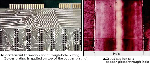
In addition, electroplated copper film also serves to suppress the deformation of plastic substrates that expand with heat. Furthermore, all substrates of a multilayer printed circuit board need to be electrically connected. Therefore, through-hole plating (i.e. creating a circuit by plating the interiors of tiny holes) is generally carried out.
In this case, the through-hole plating must meet the requirements for reliability, as it affects the nature of a printed circuit board.
Requirements for copper plating film of plated through-holes are as follows:
| 1. | Excellent throwing power (uniform plating thickness) | |
| 2. | Excellent elongation and tensile strength of the plated layer | |
| 3. | Excellent preservability (in case where no other plating is applied on top of the copper) | |
| 4. | Excellent solderability | |
| 5. | Excellent excoriation resistance |

- Environmental conservation
- Hot Dipping
- Anodic Oxidation Process
- Anodic oxidation treatment
- Anodizing
- Corrosion - Corrosion Protection
- Electroless Plating
- Electroplating
- Heat treating
- Hydrogen embrittlement
- Metal cleaning
- Metal etching
- Painting
- Special paints
- Surface Treatment
- Surface-treated steel sheets
- Thermal Spraying


Please visit your Regional MISUMI website for additional information or to request our latest catalog.
Unauthorized reproduction is prohibited by all applicable laws and is subject to criminal prosecution.