January 2013 Archives

#147 Principle of Electroplating

| No Comments | No TrackBacks

How are the electroplate coating created? Simple explanation of the principle is as follows.

Fig 1

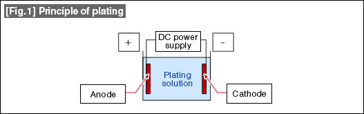
As shown in [Fig.1], the product to be plated is placed in a solution containing the ions of the plating metal as the cathode (-) ,and with an anode (+) made of the plating metal (soluble anode), then an appropriate DC voltage is applied from a power supply between both poles. As a current flows, a reduction reaction occurs at the cathode and precipitates the plating metal and the plate coating grows.

(Note 1) What is Soluble Anode?
It is a type of anode that the metal dissolves in the plating solution as the process progresses. This supplements the consumed ions within the plating solution. If the precipitated plating metal at the cathode and dissolved metal at the anode are equal in the amounts, the metal amount in the solution does not vary and is ideal. (Copper plating, etc.)

On the other hand, anodes that do not dissolve in the plating solution (Insoluble anode) is also used. In this case the metal ion is supplied by chemicals. (Chrome plating, etc.)

(Note 2) What is Reduction Reaction?
It is a reaction where the metal ions within the solution (the state which the metal is dissolved in the solution) turn into a metal on the surface of the cathode (product to be plated) by the DC current (electron) causing the ions to lose the electrical charge. An inverse of this is the oxidation reaction occurring at the anode, where the metal dissolves into the solution becoming the metal ions. Both of these cathode and anode reactions occur simultaneously.

Typically, [Plating] points to the metallic coatings applied for ornamental and anti-corrosion purposes in Japan, although the word sometimes also points to the process of applying the plate coatings itself. For instance, "This Plating is hard" would mean that the plate coating has high hardness, but "This Plating is awful" would point to the entire plating process including pre-plating polishing as well as the post plating processes.

#146 JIS Standards on Electoless Copper Plating

| No Comments | No TrackBacks

(1) Applicable range

This standard defines electroless copper plating of 5μm or more for additive method printed circuit boards (a method of using electroless copper plating to form all or part of traces on a PCB).

(2) Types of additive methods

There are following additive methods.

1. Full Additive Method

A production method using only the electroless copper plating on adhesive applied and drilled laminated substrates to produce wiring traces on planar section and through-hole section.

2. Semi-additive Method

A method of forming planar and through-hole circuit sections by applying electroless copper plating first, then electroplating and etching on adhesive applied and drilled laminated substrates.

3. Partial Additive method

Copper clad boards are etched to form the copper circuit traces, then a plating resist pattern and electroless copper plating is applied only on the through-hole section to form the circuits.

4. Panel Additive Method

A method of using copper clad boards where the boards are drilled, electroless copper plating is applied on the entire surface including the through-hole section, then unwated copper sections are etched away to form the planar and through-hole circuits.

5. Pattern Additive Method

A copper clad board is drilled, plating resist is applied, the planar and through-hole sections are electroless copper plated, then any unwated planar sections are etched away to form the circuit traces.

(3) Grades of platings

Plating grades are classified into 2 grades based on mechanical properties as shown in [Table 1].

[Table 1] Electroless Copper Plating Grades and Mechanical Properties
GradesBase SubstratesTensile strengthElongationBending stress characteristicsNotes
Class 1Copper clad boards, Adhesive applied laminated boards, Ceramic substrates, etc.195N/mm2 or more3% or more400 times or moreGeneral purpose
Class 2295N/mm2 or more7% or more800 times or moreHigh reliability purpose

(4) Plating standards

Purity of the copper used must be 99.2% or higher based on an electrochemical purity test.

(5) Density of the plating

The copper density must be 8.7g/cm3or higher based on density test.

(6) Volume resistivity of the plating

The volume resistivity must be 2.5μΩ・cm or less at 20℃.

(7) Creation method of test specimen

The test specimen for plating purity, density, volume resistivity, tensile strength, elongation, and bending stress tests are to be of 300×300mm×0.2〜1.0t stainless steel substate, 30〜35μm electroless nickel plated and delaminated. It is to be dried for 10 minutes at 50℃ or lower after the plating.

(8) Symbols

●ELp-GE/Cu25 [1]

25μm thick class 1 electroless copper plating on glass cloth based epoxy resin copper clad substrates.

●ELp-GE/Cu35 [2]

35μm thick class 2 electroless copper plating on alumina ceramic substrates.

#145 Electroless Plating, Electroless Nickel Plating - 2

| No Comments | No TrackBacks

Many characteristics can be expected for the Electroless Ni-P Alloy plate coating. The differences in the characteristics are based on the plating baths and conditions, but the diffferences can be made clear by classifying by the P contents in the coatings as shown in [Table 1]

[Table 1] Electroless Ni-P plating characteristics based on P contents
 Low P TypeMedium P TypeHigh P Type
P content in coating2〜4%8〜10%11〜13%
Crystalline structurePrecipitated stateCrystallineAmorphousAmorphous
300℃, 2hrs. laterCrystallineCrystallizedAmorphous
Magnetic PropertiesPrecipitated stateMagneticNon-magneticNon-magnetic
280℃, 2hrs. laterMagneticMagnetizingNon-magnetic
HardnessPrecipitated state700550500
Max. hardness Hv (after heat treating)950(300℃×1hr)950(400℃×1hr)950(450℃×1hr)
Corrosion resistance (Salt spray test)Somewhat inferiorGoodNormal~Good
Acid resistanceInferiorNormalGood
Alkali resistanceGoodNormalInferior
Wear resistanceGoodNormalNormal
Electrical resistivity30〜60 μΩ・cm60〜75 μΩ・cm150〜200 μΩ・cm
Temperature coefficient of electrical resistance1000 ppm/℃300 ppm/℃100 ppm/℃
Density8.6 g/cm37.9 g/cm37.6 g/cm3
SolderabilityNormal~GoodNormalNormal
Melting point880〜1300℃880〜1000℃880〜950℃
Adhesion to special materialGoodNormalNormal

The low P type with P content of around 3% has hard coating and good alkali resistance. Since it has good adhesion to special material such as ITO, polyimides, and glass, therefore used on electronic components, valves, and composite plating, etc.
The medium P type with P content of around 9% has been in long use, and this type often represents Electroless Nickel Plating when spoken of. With stable bath, it is characterized with fast precipitation, good adhesion, and good corrosion resistance.
The high P type with P content of 12% or more is known for being used as base plating of hard disk substrates due to being non-magnetic. It is also used as the resistive material for ceramic resistors due to its low temperature coefficient of electrical resistance, as well as for acid resistant components.

There are other electroless nickel platings with boron hydride compounds (Normally DMAB Dimethyl-amino-boron). Ni-B alloy platings do not easily form oxidation films on coating surfaces thus do not discolor when heat treated, has good solder adhesion, has very low electrical conductivity compared to Ni-P alloy plating. But since the baths are unstable and difficult to well manage and expensive, they are typically used on rather special purposes such as semiconductors and electronic components.
写真

月別 Archives

Pages

Powered by Movable Type 6.0.3

About this Archive

This page is an archive of entries from January 2013 listed from newest to oldest.

December 2012 is the previous archive.

February 2013 is the next archive.

Find recent content on the main index or look in the archives to find all content.